Day in the life of
Process Development Scientist – Dr. Scott R. Hammond

I’m the Director of Process Development at Nonlinear Materials Corporation.
My days vary widely. Generally, most of my time is spent in the lab, preparing, measuring, or testing samples and devices with a couple of hours of email and internal or external meetings and reporting. My lab time involves preparing samples and devices, developing new processes, measuring samples and device performance, and planning and executing new experiments.

In the lab running analysis on instruments
Specifically, this includes preparing solutions of our organic electro-optic (OEO) materials, coating thin films of OEO materials, measuring optical properties of the OEO materials, depositing electrodes and charge barrier layers via physical vapor deposition, performing electric-field poling of the OEO materials, and testing the electro-optic activity (performance) of the OEO materials and devices. When our OEO materials are hybridized with traditional silicon semiconductors, they create chips that have higher bandwidths, are smaller in size, and more eco-friendly.
Pros
The pros of my job include working in an exciting field on potentially game-changing technology (silicon-organic hybrid and plasmonic-organic hybrid nanophotonic devices) in a dynamic, scientist-driven company. I have enormous freedom to pursue the avenues of research that I think are most important to the success of the company and technology. Due to the wide range of projects underway, I am constantly performing new activities. This ensures the job never gets boring.
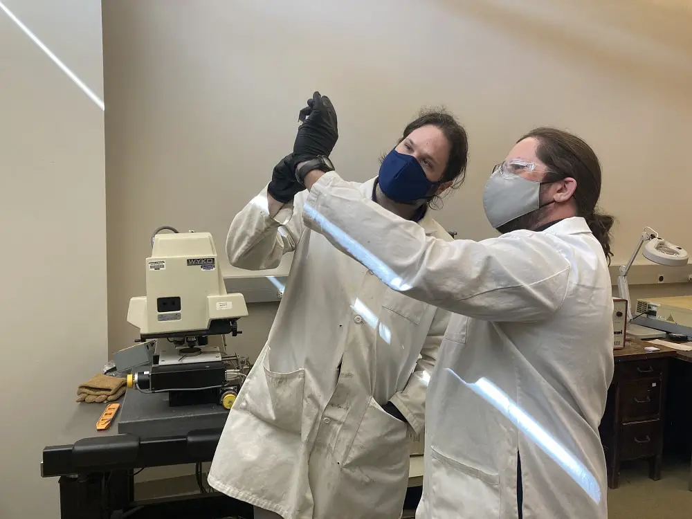
With another scientist Dr. Kevin O’Malley
Cons
The primary con is that working in a cash-strapped startup means I do not always have the resources necessary to perform all of the experiments that I would like to. I must make the best use of the limited time, equipment, and supplies available to push the technology forward as fast as possible to demonstrate its promise to the world.